Sumitomo and Co-Creation—Articulating a Vision—
Nissin Electric
Many of the smartphones used around the world feature organic light-emitting diode (OLED) displays that deliver vibrant colors. OLED displays produce high-resolution images using thin-film transistors (TFTs) formed on a glass substrate to control the light emission of individual pixels. The TFT fabrication process requires equipment that uniformly implants ions such as phosphorus and boron into a substrate.

Nissin Ion Equipment, based in Kyoto City, Kyoto Prefecture, is a wholly owned subsidiary of Nissin Electric. Its ion implanters for flatpanel display (FPD) manufacturing have a 100% global market share for sixth-generation (G6) glass substrates. In June 2025, Nissin Ion Equipment shipped the first unit of its new iG8 ion implanter, designed to handle Generation 8.6 (G8.6) extra-large glass substrates measuring 2,290 mm long and 2,620 mm wide. The iG8 is enormous—roughly the size of a tennis court, with its highest point reaching 5.5 meters.
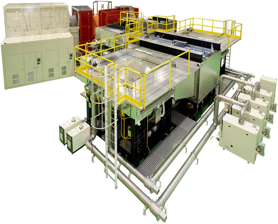
The need for the new equipment stems from significant technological changes in the display industry. Display technology has evolved from liquid crystal displays (LCDs) to self-emissive OLEDs, while TFT technology has progressed from amorphous silicon TFTs to low-temperature polysilicon (LTPS) TFTs, which enable higher-resolution displays, and then to energy-efficient oxide semiconductor TFTs typified by IGZO, a material composed of indium (In), gallium (Ga), zinc (Zn), and oxygen (O).
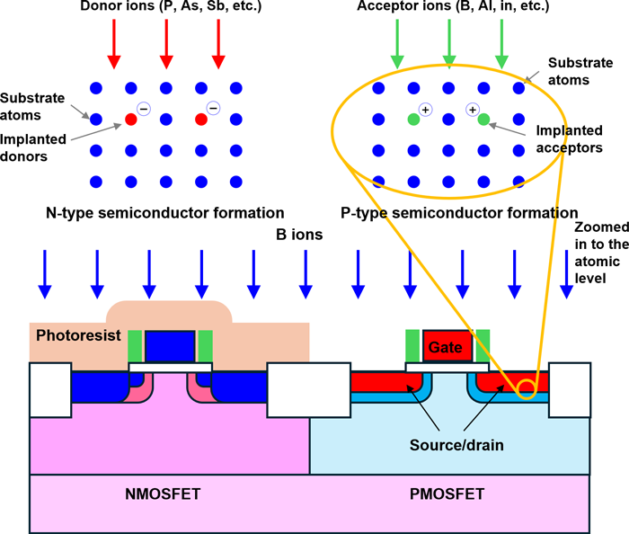
LCDs once dominated the market, with Nissin Ion Equipment and other companies competing to advance their technologies. However, the widespread adoption of OLEDs for smartphones created demand for higher-performance TFTs capable of supporting higher-resolution displays. To meet these requirements, the performance of LTPS-TFTs for OLEDs was enhanced, and customers began adopting PMOS transistor structures because of their high current-drive capability and advantages in manufacturability and device performance.
Even before this trend gained momentum, Nissin Ion Equipment had been developing high-current boron ion implantation technology to support the adoption of CMOS structures for higher-performance LTPS-TFTs. The company’s expertise, cultivated over many years, aligned with the technical requirements of the market, enabling it to achieve a 100% global market share in ion implanters for G6 substrates. This success reflects not merely the company’s response to changes in the market, but also its sustained R&D efforts in anticipation of future technological advances.
Nissin Ion Equipment’s strength lies not only in its technological superiority but also in its commitment to supporting customers beyond the sale of its equipment. If a problem arises after equipment delivery, the company listens carefully to its customers and works with them to identify the cause, even if the problem lies outside the scope of its own equipment. By engaging sincerely with customers in this way, Nissin Ion Equipment has cultivated trust over the years.
At first glance, the new G8.6-compatible iG8 ion implanter appears to have been developed to accommodate larger substrates. However, its development actually originated in efforts to apply ion implantation to oxide semiconductor TFTs, which are considered one of the promising technologies for next-generation displays.
While oxide semiconductor TFTs are widely used for large displays, they have generally been considered a technology that does not require ion implantation. However, Nissin Ion Equipment has been conducting research and evaluation for many years based on the idea that ion implantation could enable miniaturization and improved reliability.
Furthermore, the adoption of OLED technology is expected to accelerate beyond smartphones to larger-screen IT devices such as laptops, tablets, and monitors. To improve production efficiency for these products, the display industry is transitioning to G8.6 substrates, making the ability to accommodate larger substrates essential for meeting market needs. In other words, the iG8 is not simply an ion implanter designed to handle larger substrates; it is an extension of the company’s R&D efforts toward realizing next-generation display technology.
The rapid adoption of artificial intelligence (AI) has also provided a boost to development. The enormous amount of processing required by the explosive growth of AI consumes vast amounts of power. Currently, prompts (instructions) entered on a device are sent to AI servers for processing, but many users are reluctant to send personal information and other sensitive data to external cloud servers. If “on-device AI,” which processes such information locally on a user’s smartphone rather than sending it to the cloud, becomes widespread, the overall power consumption of devices will increase, creating an even greater need for energy-efficient displays.
Technologies for reducing display power consumption include low-temperature polysilicon oxide (LTPO), which is rapidly being adopted in smartphones and other devices. Nissin Ion Equipment’s ion implantation technology can be applied to both oxide semiconductor TFTs such as IGZO and to LTPO devices. Furthermore, although several ion species are candidates for implantation into oxide semiconductors, the company’s research has confirmed that boron is one of the most promising options. The boron implantation technology developed since the LTPS era is thus also applicable to next-generation TFT technologies. Developed with future support for IGZO in mind, the iG8 is well positioned to benefit from two major trends: growing demand for LTPO and the drive for greater energy efficiency in the age of AI.
From semiconductor manufacturing and display production to material modification, Nissin Ion Equipment continues to explore new possibilities for ion beam technology, creating value for future industries and society.
A prime example is KYOKA, unveiled in December 2023 as the world’s first mass-production system dedicated to material modification. By employing ion beams to precisely tailor surface characteristics, the technology enables control over a wide range of material properties, including optical performance, electrical functionality, corrosion resistance, and the selectivity and rate of subsequent etching processes. Through these capabilities, KYOKA is expected to open new pathways for next-generation manufacturing, including applications in advanced semiconductor processes requiring ever-greater precision.
Building on ion beams as its core technological platform, Nissin Ion Equipment continues to expand the horizons of their application. The company’s journey has progressed from semiconductor device manufacturing to display production, and now further into the field of material modification, creating new value by applying its expertise to increasingly diverse industrial challenges.
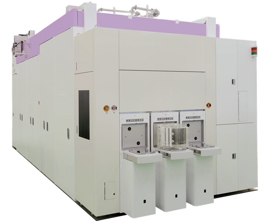
Throughout its history, Nissin Ion Equipment has anticipated major technological shifts and responded with innovation. As display technologies evolved from LCD to OLED, and thin-film transistor technologies advanced from LTPS to oxide semiconductors, the company developed distinctive solutions that enabled it to remain at the forefront of the industry. Today, it is applying the same forward-looking approach to emerging fields such as material modification.
Rather than merely adapting to changes in the marketplace, Nissin Ion Equipment seeks to look beyond them, identifying the technological challenges that future industries and societies will face. Through the power of ion beams, Nissin Ion Equipment will continue to create technologies that contribute to society and help realize a more prosperous future.
 Journalist Shumon Mikawa on Sumitomo’s DNA
 EN
EN